Driving a shift register using an AVR chip’s built-in hardware is really quite easy. Most of their offerings have an SPI module, or Serial Peripheral Interface. A shift register is exactly that, a peripheral device that communicates via a serial line. All we need to do is hook up our connections and use a few pieces of simple code. Join me after the break to see how that’s done.
Just want to know how shift registers work? Check in on my other post on that topic.
Schematic
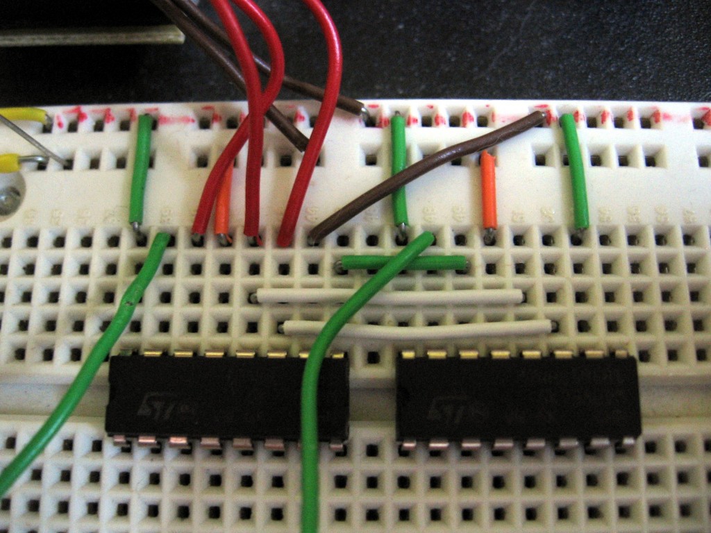
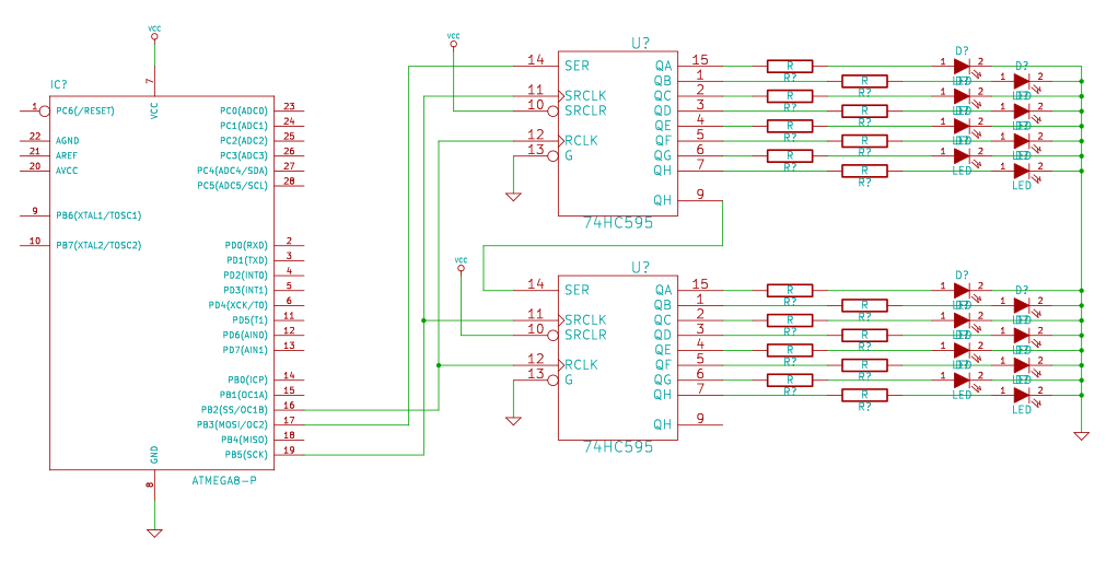
The first thing to consider is that it may not be necessary to connect the Clear and Enable pins to the microcontroller. If there are relatively few shift registers being used together it may be easier to shift in all zeros and latch them to the registers. But if timing is a big issue you may want this capability. For this example I have just connected the SCLR pin to VCC and the enable pin to GND.
This leaves three control pins: SI, SCK, and RCK. It is possible to drive SCK and RCK from the same signal, but that’s for another tutorial. My test hardware, the ATmega168, has pins meant to drive each of these controls. Note that the serial and storage clocks (SCK and RCK) for both shift register chips are hooked together on two data buses. The Serial In of the first chip (SI) is connected to the microcontroller. The QH prime pin of this first chip is connected to the SI pin of the second chip to cascade the data from one to the next.
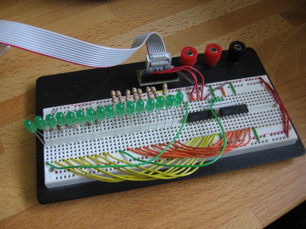
 Test hardware. The ATmega is connected via the ribbon cable.
Using the AVR SPI hardware
Accessing the SPI hardware is pretty simple. There’s only a few things that need to happen to get it running:
- Define which pins we’re using and set them to outputs
- Enable SPI and set it to Master mode
- pull the SS pin low
- Write our data to the SPDR, it will automatically be strobed into the shift registers
- Toggle the latch to display the data on the LEDs
The definitions are easy enough. I can’t just choose any pins, the SPI outputs are specific pins which can be looked up in the datasheet:
#define SHIFT_REGISTER DDRB
#define SHIFT_PORT PORTB
#define DATA (1<<PB3)           //MOSI (SI)
#define LATCH (1<<PB2)          //SS   (RCK)
#define CLOCK (1<<PB5)          //SCK  (SCK)
  SHIFT_REGISTER |= (DATA | LATCH | CLOCK);     //Set control pins as outputs
  SHIFT_PORT &= ~(DATA | LATCH | CLOCK);                //Set control pins low
Enabling SPI in Master mode is a one-liner. But there are other clock prescaling options that you can choose from if you need to. I’ll leave that up to you to explore:
SPCR = (1<<SPE) | (1<<MSTR); //Start SPI as Master
The SS pin can be pulled low as normal. What I find interesting is that Atmel’s example code in the ATmega168 datasheet doesn’t include this step. You have to really read the SPI section to get at the important nugget: “When configured as a Master, the SPI interface has no automatic control of the SS line. This must be handled by user software before communication can start.”. We can handle that:
//Pull LATCH low (Important: this is necessary to start the SPI transfer!)
 SHIFT_PORT &= ~LATCH;
Now we write our byte to the SPI Data Register. The chip’s hardware takes it from here. You want to make sure it’s done shifting out data before sending any more so we use a while loop to check a flag which will be set when the hardware has finished:
  //Shift in some data
  SPDR = 0b01010101;            //This should light alternating LEDs
  //Wait for SPI process to finish
  while(!(SPSR & (1<<SPIF)));
Finally, the LEDs won’t light up until the data is latched into the storage register:
  //Toggle latch to copy data to the storage register
  SHIFT_PORT |= LATCH;
  SHIFT_PORT &= ~LATCH;
The finished program looks like this:
#include <avr/io.h>

#define SHIFT_REGISTER DDRB
#define SHIFT_PORT PORTB
#define DATA (1<<PB3)		//MOSI (SI)
#define LATCH (1<<PB2)		//SS   (RCK)
#define CLOCK (1<<PB5)		//SCK  (SCK)

int main(void)
{
  //Setup IO
  SHIFT_REGISTER |= (DATA | LATCH | CLOCK);	//Set control pins as outputs
  SHIFT_PORT &= ~(DATA | LATCH | CLOCK);		//Set control pins low

  //Setup SPI
  SPCR = (1<<SPE) | (1<<MSTR);	//Start SPI as Master

  //Pull LATCH low (Important: this is necessary to start the SPI transfer!)
  SHIFT_PORT &= ~LATCH;

  //Shift in some data
  SPDR = 0b01010101;		//This should light alternating LEDs
  //Wait for SPI process to finish
  while(!(SPSR & (1<<SPIF)));

  //Shift in some more data since I have two shift registers hooked up
  SPDR = 0b01010101;		//This should light alternating LEDs
  //Wait for SPI process to finish
  while(!(SPSR & (1<<SPIF)));

  //Toggle latch to copy data to the storage register
  SHIFT_PORT |= LATCH;
  SHIFT_PORT &= ~LATCH;

  while(1)
  {
	//Loop forever
  }
}
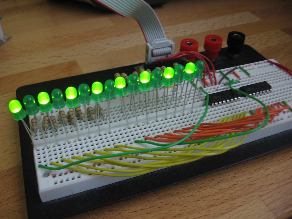
And here’s what my hardware looks like once I flash it to the chip:
Moving beyond
This video shows the result of my hardware setup used as a binary counter. I moved all of the useful commands into functions, set up a delay in the loop, and typecast an Int that gets incremented during each loop in order to shift it out to the registers. Check out my Github repository to see how that was done.
It gives you a bit of an idea of where you can go from here. For me, this was just a stopping point before I move my Larson Scanner to an expandable shift-register design and transition away from PWM for a more efficient BCM. Check back soon for that post!


