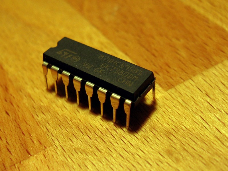
Shift Registers are integrated circuits that take a serial input and turn it into a parallel output. This is extremely valuable if you need more input/output pins than your microcontroller has available. For hobbyists the most common use is driving LEDs with a 595 shift register. Let’s look at how this is done.
After the jump I’ll discuss control methods, and I’ve assembled a video that illustrates the functions of a shift register.
Grab a copy of a datasheet for a common shift register, like the ST M74HC595 (PDF). I’ll walk you through the logic diagram on page 2:
Shift Register Have Three Main Parts
As you can see in the diagram above, there are three main parts to this shift register shown as three large rectangular boxes. The top is the shift register itself, which passes one bit at a time from the input (Serial In or SI) down each of the eight bits until it pops out of the serial output (QH prime). A clock (SCK) signal determines when each shift happens.
Each bit on the shift register can be copied into the storage register. This is done using a separate clock signal (RCK). This clock signal is often called a latch.
When data is latched from the shift register into storage register it appears on the 3-State Buffer as long as it is enabled (G held low). Here you can see that the 8-bits of data will appear on output pins QA through QH.
Five Control Inputs
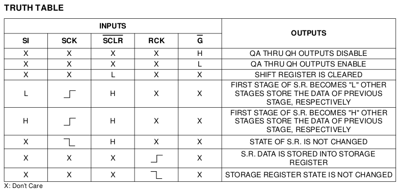
There are five control pins on this type of shift register:
- Serial In (SI): The logic value of this pin will be moved into the shift register the next time the Shift Register Clock (SCK) goes high
- Shift Register Clock (SCK): This causes all of the bits in the shift register to move one space over. The logic value of SI takes the empty space, and the value that is pushed off the other end of the shift register appears on the Serial Output (QH prime)
- Shift Register Clear Input (SCLR): This input clears all of the data stored on the shift register (as well as the Storage Register). This happens when the SCLR is driven low. Hold the pin high when shifting data into the device or it will be immediately cleared.
- Storage Register Clock (RCH): When driven high this pin copies the data in the shift register to storage register. Part of the brilliance of the 595 chip is that you can move data into the chip, then display it on the outputs only when everything is in place just by toggling this pin.
- Output Enable (G): I often call this pin E because G makes no sense to me. Basically, if you drive this pin high it will turn off the outputs. The data is still kept safe in the storage register, it’s just not being shown on the output register pins. This can be used for blinking LEDs, and if you do it right, dimming them via Pulse Width Modulation.
The Workings of a Shift Register
I’ve made a video that outlines how this chip functions. Take a look and get ready to use the pause button as you may want to study the state of the registers before each clock signal. A couple of things that will help you understand what’s going on:
- When shifting data, the bit of “Input Data” currently being written is highlighted in red.
- The QH box is referring to the Serial Output pin (QH prime).
- What you see is the state of the external pins on the chip. The internal shift register and storage register data is not show. A good exercise would be to track the status of those two registers during each step of the video by using a pencil and paper.
Explanation of Function
Here’s an overview of the various functions seen in the video:
- Data is shifted into the chip by setting the appropriate logic level (0 or 1) on the SI pin, then toggling the clock (starting low, then to high and back to low). It will proceed by adding one bit per clock cycle until the shift register is full (8 clock cycles in this case). Data pushed off the other end of the shift register will appear on the QH prime pin which can be used as the serial output for the next chip. This feature is often called ‘cascading’.
- Once there is data in the shift register it can be saved in the storage register by toggling the Storage Register Clock (RCK or ‘latch’). This data will appear on the outputs as long as the enable pin (G) is held low.
- The outputs can be turned on and off without affecting the storage register. Drive G high to disable outputs and low to enable them.
- The chip can be driven with as little as two signals if SCK and RCK are both driven together (the second signal would be the incoming serial data line). With this technique, the values of the storage register will be one bit behind the values of the shift register.
- The serial register can be cleared by pulling the SCLR pin low. This will not clear the storage register, so an additional latch (toggle RCK) will be necessary to clear it (this has the effect of clearing the outputs too).
One note about driving SCK and RCK together. If you have LEDs connected to the outputs you will see the bits shifting into the chip (perhaps incredibly fast but you’ll still see something). This may be okay with you, but if you’re using the outputs to drive other devices it may be a problem.
Conclusion
This is the theory behind the operation of a 595 shift register. But you may want to actually hook one up and do something with it. Don’t worry, there are tutorials for that as well:
- Operating shift registers using hardware (SPI)
- [COMING SOON] Operating shift registers using software (bit banging)


